
Every silicon launch that misses its window has a common culprit pattern: the SDK was outsourced to a partner with the right CV and the wrong capability.
This article captures ten lessons that chipmakers learn late in their semiconductor development programmes, about platform scope creep, PTS debt, Docker delivery failures, Channel Sounding IP gaps, and the cost of skipping standards contribution. Each lesson carries a concrete cost estimate and a brief on what correct looks like. A self-scoring checklist at the end tells you how many of these risks are live in your current outsourcing brief.
Why SDK outsourcing for new silicon fails so often
Wireless SDK outsourcing is not product firmware development. When a chipmaker hands off SDK development to a wireless connectivity engineering partner, the output is not an application. It is the software layer that every chip customer will build on. The tolerance for bugs, missing features, and incompatible platform assumptions is essentially zero, because the SDK’s failures become the chip customer’s support calls, and the chip customer’s support calls become your design-win losses.
Whether you are selecting a contract R&D partner for semiconductor equipment vendors or a dedicated SDK house, the ten lessons below are not academic. Each one reflects a pattern where the contractual requirement was met (the partner delivered a working SDK) but the programme outcome was a delayed launch, a failed SDK certification, an interoperability event that exposed missing coverage, or a chip customer who put a competitor part in the next design. In each case, the risk was visible before contract signature, if anyone had known to look for it.
In 2026, the r&d semiconductor landscape includes chipmakers releasing BLE UWB, BLE 5.4, and BLE 6.0 silicon into markets where the software layer is the primary differentiator. The ten lessons that follow apply to all of them.
Lesson 1: Your partner has never worked at silicon level
The difference between a firmware engineer and a silicon SDK engineer is not language proficiency or toolchain familiarity. It is the mental model of what the software is for. A firmware engineer asks: does this feature work on this hardware? A silicon SDK engineer asks: does this API design work across every host platform our chip customers will run, including platforms that do not exist yet?
The practical consequence is this: a product-firmware company that takes your SDK contract will scope the work around the reference design you give them. When a chip customer arrives with a different RTOS, a different host processor, or a different power management constraint, they will hit the edge of the SDK’s real design. The firmware company will have met the brief. You will be on the hook for the porting work.
How this surfaces: the first chip customer support request that cannot be closed with a config change. Typically week twelve after customer SDK delivery.
What correct looks like: the partner has delivered SDK layers (not just firmware) to at least two different silicon vendors, each on multiple host platforms. They can describe how they handled the interface between the radio driver, the protocol stack, and the customer application layer. They have a porting guide that ships with the SDK as a standard deliverable.
The signal to watch for in a scoping call: ask the partner how they handle a chip customer who wants to run the BLE stack on a custom RTOS you did not test. If the answer is “we’d need to scope that,” the partner is not a silicon SDK company.
Lesson 2: Manual PTS is not an SDK certification plan; it is a certification debt
The Bluetooth SIG currently maintains over 600 test cases in the Profile Tuning Suite (PTS). Running them manually takes four to eight weeks depending on the test engineer’s experience and the defect rate on the device under test. Running them once per quarter adds up to three to six months of certification-occupied engineering time per year. On a programme where the chip architecture changes with every silicon revision, manual PTS is not a process. It is a debt you are taking on against every future revision.
The correct model is automated PTS regression: a CI/CD pipeline that runs the PTS suite (or the test-relevant subset) nightly, catches SDK certification-breaking regressions at commit, and produces a QDID-ready test report on demand. The investment to build this pipeline is front-loaded. The ongoing cost is monitoring rather than execution.
The Bluetooth SIG’s qualification programme requires a QDID for every listing. The SIG does not audit how many sprints you spent re-running test cases manually. That cost is yours.
What this costs: a manual PTS cycle that reveals a regression three weeks before launch adds six to eight weeks to the programme. An automated pipeline catches the same regression on the commit that introduced it, typically same day.
The signal to watch for: ask the partner what happens when a BLE stack change breaks a PTS test case. If the answer describes a test cycle that takes longer than twenty-four hours to detect the failure, the pipeline is manual.
Lesson 3: You scoped the SDK for one platform and discovered three more at the demo
Silicon vendors discover their target markets late. A chip that was designed for smart locks signs its first design win with an automotive OEM. The BLE SDK scoped for nRF52 must now run on an Infineon PSoC microcontroller and an NXP i.MX host. The partner who built the SDK for a single platform now has a porting contract to negotiate under programme pressure.
This is not an edge case. It is a routine pattern in chipmaker programme history. The solution is not to scope for all platforms in advance (that is not possible in contract round one). The solution is to choose a partner whose SDK architecture makes porting to a new platform a three-week task rather than a three-month rewrite.
The architectural requirement is clear: the SDK must have a hardware abstraction layer (HAL) that cleanly separates the radio driver, the protocol stack, and the application API. If the partner has not designed the HAL with platform portability as a first-class constraint, every new platform is a near-full rewrite.
What this costs: a platform porting contract on a poor HAL design costs three to five months of engineering plus a QA cycle. A porting task on a well-designed HAL costs three to four weeks.
The signal to watch for: ask the partner to show you the HAL boundary in a shipped SDK. If they cannot point to a clean abstraction layer, assume the porting cost is three months per new platform.
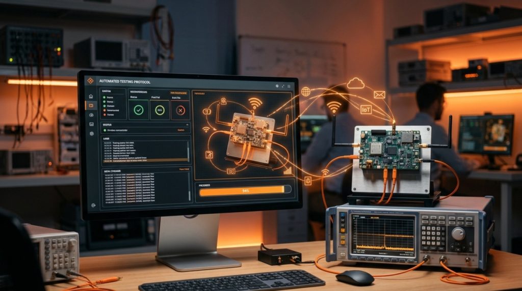
Lesson 4: The BLE 6.0 Channel Sounding spec does not include the ranging algorithm
BLE 6.0 Channel Sounding is one of the most commercially significant additions to the Bluetooth standard in a decade. It enables sub-metre ranging (sub-decimetre with the right implementation) using the BLE radio already present in billions of devices. Chipmakers releasing BLE 5.4 chips today and planning BLE 6.0 Channel Sounding silicon for next year are under competitive pressure to demonstrate centimetre accuracy at launch.
Here is what the BT SIG specification actually provides: a tone exchange mechanism, a phase measurement method, and a frequency hopping sequence. What it does not specify is the ranging algorithm: specifically, the Phase-Based Ranging (PBR) solver that converts raw phase measurements into a distance estimate. The integer-ambiguity problem (where the same measured phase corresponds to multiple possible distances) is the core engineering challenge. Solving it well is the difference between “sub-metre in a clear corridor” and “15 cm in a multi-path environment.”
No NXP, Texas Instruments, Infineon, or Qorvo internal team has this solved as a customer-deliverable software module. The FiRa Consortium’s certification programme validates UWB interoperability but does not prescribe BLE ranging algorithm quality. The ranging performance that appears in your marketing collateral is your partner’s algorithm, not the standard’s.
What this costs: a chipmaker who ships without a high-quality PBR solver loses Channel Sounding design wins to competitors with better ranging performance, typically two to four design win cycles before the gap is closed or a better algorithm is licensed.
The signal to watch for: ask the partner to describe their PBR solver. Specifically, ask about integer-ambiguity resolution. If the answer is “we implement the BT SIG spec,” they do not have a solver. The spec is necessary but not sufficient.
Lesson 5: The SDK delivered as a tarball is your chip customers’ first support call
The most common SDK delivery model in the industry is a compressed archive: source code, a Makefile, and a README. This model is a product of an era when chip customers had stable, homogeneous build environments. That era ended around 2018. A chip customer in 2026 is running Linux distributions that update every six months, Python environments managed by conda or pyenv, and cross-compilation toolchains that conflict with each other if the versions are not pinned.
A tarball SDK that builds cleanly on your partner’s Ubuntu 22.04 machine may break on the customer’s macOS 14 machine, the customer’s Windows Subsystem for Linux environment, or the customer’s internal CI runner with a different GCC version. Each of these failure modes generates a support ticket.
The correct delivery model is a Docker container: a defined base image, compiler version, linker, and SDK source pinned to specific digests, delivered as a single docker pull. The customer runs one command. The build either works or the failure is inside the container: reproducible, debuggable, and independent of the customer’s host environment.
What this costs: SDK support from a tarball-delivered project averages two to four hours per chip customer in the first six months. Across twenty chip customers, that is eighty to one hundred and sixty FAE hours before any actual bug is found. Docker delivery reduces this to near zero for build environment failures.
The signal to watch for: ask the partner how their SDK is packaged for customer delivery. If the answer does not include “Docker” or “reproducible build system,” assume tarballs and budget the FAE hours accordingly.
Lesson 6: Testing against your own reference stack tells you nothing about field interoperability
A UWB SDK that passes all of its own unit tests and interoperates perfectly with its own reference design can still fail at a FiRa plugfest when it encounters an Apple, Qorvo, or NXP device. This applies across every protocol where a compliance programme exists.
The test that matters for field interoperability is: does your SDK communicate correctly with a device running a completely independently implemented stack? Not a different version of your stack. Not a stack that shares code modules. An independently written stack from a company that made different implementation choices at every ambiguous point in the specification.
Very few SDK partners have this test infrastructure. Running it requires either a library of reference devices (Apple UWB hardware, Qorvo DW3xxx evaluation kits running competitor firmware, NXP SR040 boards, Android devices with Jetpack UWB) or a UWB Protocol Sniffer capable of decoding and analysing frames from any manufacturer’s radio, not just the client’s silicon.
What this costs: a FiRa CCC interoperability event failure that exposes a protocol-layer incompatibility adds three to six months to the certification timeline. The failure is in the spec interpretation, not the hardware. Diagnosing which party’s interpretation is wrong requires frame-level analysis of a packet exchange between two devices, exactly what the Protocol Sniffer provides.
The signal to watch for: ask the partner what other companies’ stacks they test against. If the answer is “we test against the client’s reference design,” they test against themselves.
Lesson 7: SDK certification scope creep is the most expensive delayed discovery in semiconductor development
A chipmaker releasing a multi-standard chip (BLE 5.4, Thread 1.3, and Wi-Fi 6 on the same die) needs three separate semiconductor certificate pipelines: BT SIG / PTS for the BLE stack, the Connectivity Standards Alliance (CSA) for Thread and Matter certification, and the Wi-Fi Alliance for Wi-Fi qualification. Each pipeline has its own test plan, its own certification body relationship, its own QDID or semiconductor certificate listing format, and its own update cadence when the spec revises.
It is common for chipmakers to scope only the primary protocol’s SDK certification in the initial contract and treat the others as “to be scoped later.” Later typically arrives when the sales team has signed a design win that requires the semiconductor certificate the programme did not fund.
The Connectivity Standards Alliance now governs Matter, Thread, and Zigbee certification in one umbrella, meaning a chip that ships into a smart home ecosystem must satisfy CSA requirements across potentially three protocol stacks. This is a full-time programme management workstream, not a three-week effort at the end of the project.
What this costs: an unscoped SDK certification requirement discovered after silicon tape-out adds four to twelve months to the launch, depending on whether the required test infrastructure already exists in the programme.
The signal to watch for: at contract signature, the SDK certification scope should name every standards body that will issue a qualification listing for your chip, including the specific programme (BT SIG QDID, FiRa CTF, CSA DCL, Wi-Fi Alliance CWID), and the responsible partner or internal team. If any of these are listed as “TBD,” they are out of scope.
Lesson 8: Chip bring-up speed determines whether you hit your launch window
Most engineering services companies have a stated ramp time of “two to four weeks.” This is the time from contract signature to the first engineer appearing in your Jira board. The actual time to first useful technical contribution (first build on your silicon during chip bring-up, first ranging packet, first PTS test run) is often twelve to twenty-four weeks, because the engineers assigned to your programme are ramping on your chipset’s architecture, your radio subsystem, your build environment, and your internal technical context simultaneously.
On a chipset programme with a six-month window to first customer SDK delivery, a twenty-four-week silicon bring-up period leaves four weeks for actual SDK development. This is not a hypothetical. It is a pattern that repeats in every semiconductor development programme that sources a new partner without requiring evidence of existing familiarity with the radio architecture.
What correct looks like: an SDK partner who has already worked with the same radio architecture can complete chip bring-up in two to four weeks because they already understand the transceiver register map, the timing characteristics, and the protocol layer quirks. The ramp cost is absorbed by their prior experience rather than by your launch timeline.
The signal to watch for: ask the partner: “What is the name of the last chipset you brought up, and what was the time from first silicon to first ranging packet?” If they cannot name a specific chipset and a specific time, they have not done chipset bring-up in the sense your programme requires.

Lesson 9: Treating standards contribution as a vendor’s problem is a chipmaker’s mistake
The temptation for a chipmaker is to treat standards body participation as someone else’s job. “We implement the standard; the standard is defined by others.” This is a reasonable approximation in a stable protocol environment. It is not a reasonable approximation in UWB, BLE 6.0, and Matter in 2026, where the relevant specifications are all in active amendment cycles.
IEEE 802.15.4ab, the UWB amendment adding enhanced ranging, pulse shaping, and interference robustness, is in active development. The working group meets quarterly and produces technical contributions that directly affect the interoperability requirements an SDK must satisfy. A chipmaker whose SDK partner is not in the room when those contributions are agreed finds out about the resulting interoperability change at the next plugfest, not at the standards meeting.
The practical benefit of a partner who contributes to the spec is not prestige. It is early draft access, which means the SDK tracks the spec before publication rather than after. It is influence over the test plan, which means fewer specification ambiguities are resolved against your implementation at an interop event.
What this costs: a chipmaker who ships a UWB SDK without standards-aligned interoperability typically fails the first FiRa plugfest at one or two points where the spec was ambiguous and the implementation made the wrong choice. Plugfests happen quarterly. The cost is three to six months.
The signal to watch for: ask the partner to name the standards body contributions they have made in the past twelve months. If the answer is vague (“we track the standards”) or focuses only on implementation (“we implement the FiRa spec”), the partner is a consumer of standards, not a contributor.
Lesson 10: An SDK without versioning discipline is a support contract that never ends
The final lesson is the one most often discovered not by the chipmaker but by the chip customer. SDK versioning discipline means: every release has a version number, a changelog, a migration guide from the previous version, and a deprecation policy for APIs that are being removed. It means that a chip customer who upgrades from SDK version 2.1 to version 2.2 can read a document that tells them exactly what changed, what broke, and what they need to update in their application.
What chipmakers routinely receive instead is an SDK in which the version number increments but the changelog is a Git commit log. The chip customer who needs to upgrade to pick up a certification-breaking bug fix must diff the source code to understand what changed.
What correct looks like: the SDK ships with CHANGELOG.md, MIGRATION.md for each minor version bump, API deprecation notices in the source with a timeline for removal, and a support lifecycle table that tells chip customers when a version goes end-of-life.
The signal to watch for: ask the partner for an example changelog from a previous SDK delivery. If they produce a Git log, the documentation practice is absent. If they produce a structured changelog with semantic version numbers and migration guidance, the practice exists.
Self-scoring checklist
Score one point for each question that describes your current outsourcing brief or the partner you are evaluating. Maximum 10.
- The partner has delivered a completed SDK (not firmware or a demo) to at least one other silicon vendor
- The partner runs automated PTS regression; test results are available within twenty-four hours of a commit
- The SDK scope document names the host platforms to be supported on day one (minimum three)
- The partner has described their Channel Sounding / PBR solver specifically, not with reference to the BT SIG spec
- The SDK delivery model specifies Docker-based packaging for chip customer distribution
- The partner has tested their stack against at least one independently developed competitor stack
- The SDK certification scope names every relevant standards body and programme (BT SIG, FiRa, CSA, Wi-Fi Alliance as applicable)
- The partner has completed chip bring-up on a chipset in the same radio architecture family in under eight weeks
- The partner holds active membership in at least one relevant standards body and can name a recent contribution
- The partner’s previous SDK deliveries include a structured CHANGELOG and MIGRATION guide per release
8–10: Your outsourcing brief is well-structured. The risks in this article are either mitigated or consciously accepted.
5–7: Three to five risks are live. Prioritise the ones in C3 (Channel Sounding IP), C4 (SDK certification automation), and C7 (standards contribution). These cannot be fixed mid-programme.
3–4: Your programme has material late-stage risk. Consider adding a technical scoping session with your SDK partner before the statement of work is finalised, focused specifically on the gaps.
0–2: The current partner selection is likely to produce a delayed launch. Revisit the shortlist before contract signature.
Work with needCode
needCode builds wireless SDKs for semiconductor companies, with proprietary PBR Channel Sounding solvers for BLE 6.0, automated PTS and FiRa SDK certification pipelines, Docker-based SDK distribution, and active participation in IEEE 802.15.4, FiRa Consortium, and Bluetooth SIG. If you are outsourcing wireless SDK development for new silicon and want to avoid the lessons in this article, we are happy to talk through your semiconductor development programme and where we can reduce your programme risk.
Book a free discovery call or get in touch
Frequently asked questions
Ask for a ranging accuracy benchmark from a real environment, not a line-of-sight test range. Specifically: what is the 90th percentile ranging error at 10 metres in a multi-path indoor environment (corridors, reflective surfaces)? A partner with real PBR solver IP will quote a number, typically under 15 cm for a well-tuned solver, and can explain what algorithm produces it. A partner without it will describe the BT SIG tone exchange mechanism, which is not an answer to the question.
Yes. Ask for the name of the last chipset they brought up and request a brief (one-page) technical summary of the silicon bring-up sequence: what the first working build looked like, what the first identified issue was, and how long from first silicon to first protocol output. This document should take two hours to produce if the chip bring-up happened. If the partner cannot produce it, the bring-up claim is aspirational.
At minimum: a Bluetooth SIG QDID covering the BLE stack and the Channel Sounding feature, and a FiRa CTF listing if the chip targets the location services market. If the chip also targets Matter-based ecosystems, add CSA device certification. Wi-Fi Alliance certification becomes mandatory only if the chip includes a Wi-Fi radio. The total lead time for BT SIG plus FiRa is twelve to eighteen months with an automated SDK certification pipeline. Every semiconductor certificate your chip needs should be named in the statement of work before contract signature.
Docker is the most common and most portable answer, but the underlying requirement is reproducibility. Any build system that produces the same binary from the same inputs regardless of the customer’s host environment is acceptable: Nix, Bazel with hermetic builds, or a containerised Yocto layer for embedded Linux targets. The failure mode is any model where the customer’s host environment state affects the build output. If the build passes on your partner’s machine and fails on the customer’s machine, the model is wrong regardless of what it is called.
The direct cost is three to six months of programme delay: the time between the plugfest failure and the next FiRa plugfest where you can demonstrate compliance. The indirect cost is the design win that specified FiRa compliance as a selection criterion and is now waiting for your chip to pass. The preventable fraction is high: most plugfest failures result from spec interpretation ambiguities that are visible in advance to a partner who participated in writing the test plan or who has previously tested against the failing device type. A UWB Protocol Sniffer that can decode frames from the test device in real time converts a plugfest failure from a three-month delay into a same-day diagnosis.
Further reading
- Embedded engineering partner for semiconductor manufacturers
- BLE SDK development for chipmakers
- BLE 6.0 Channel Sounding and PBR ranging IP
- UWB Protocol Sniffer for bring-up and interop testing
Also see: Which wireless connectivity engineering partner should build your semiconductor SDK?